Let Us Know How We Can Help. We Are Your Dedicated Solutions Provider.
PCB Design Services
- Home
- PCB Design Services
PCB Design Services
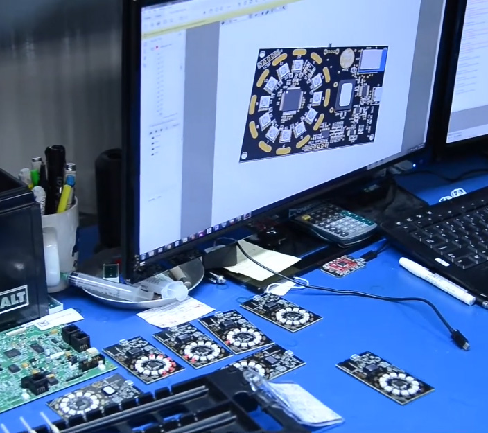
PCB design, or Printed Circuit Board design, is the process of creating a layout for a circuit board that connects electronic components using conductive tracks, pads, and other features etched onto a non-conductive substrate. It involves schematic design, component placement, routing of electrical connections, and ensuring signal integrity, thermal management, and manufacturability. The goal is to produce a functional and cost-effective board for electronic devices.
// Expert Printed Circuit Board Design
Speed Up Product Development With Trustworthy PCB Design Services
EMS, Inc. provides comprehensive services for your PCB design, layout, and manufacturing requirements. We transform your concept into a fully functional product, offering both PC Board Manufacturing and Assembly Services tailored to your needs.
Our team has designed hundreds of PCBs for a variety of electronic products and technologies. By managing every step, from the initial idea to the final assembly, we help ensure your project’s success. EMS’ comprehensive approach guarantees your design can be produced easily, cost-effectively, and reliably. We work quickly through product development, prototyping, pre-production, and full manufacturing. This all-in-one service helps deliver your product on time and within budget.
PCB Design Services Flow
- Library creation
- BOM generation
- Schematic capture
- PCB stack-up design
- PCB layout and routing design
- Gerber (DFM) validation
- Verification and simulation
- PCB manufacturing file creation
Types Of Boards We Support
- Single Sided PCB
- Double Sided PCB
- Single Layer PCB
- Multi Layer PCB
- Rigid PCB
- Flexible PCB
- Rigid-Flex PCB
- Ceramic PCB
High Speed Interfaces
- DDRx
- PCIe
- MIPI
- USB 2.0/3.0
- HDMI
- Ethernet
- XAUI
- SATA
HIGH-SPEED PCB LAYOUT DESIGN
High-speed PCB layout design is essential for today’s electronics, focusing on reducing signal integrity problems and electromagnetic interference. It involves careful planning of trace width, length, and spacing for efficient signal travel. EMS has experience creating complex PCBs using multiple layers and various signaling standards, such as SATA 6G and 10G Ethernet. The team employs advanced tools to optimize layouts, ensuring precision and efficiency while meeting industry standards and deadlines.
COMPLEX PCB LAYOUT DESIGN
We specialize in complex PCB layout design that supports multiple layers and typically encompasses over 2000+ components and nets, all within tight packaging constraints. Oftentimes, our designs may include non-standard placements to fit complex shapes and tight spaces. We focus on making sure everything fits perfectly without risking short circuits or clearance issues. This meticulous attention to detail enhances performance and reliability, making our solutions ideal for advanced electronic applications.
// Most Frequent Questions
PCB Design FAQ
PCB (Printed Circuit Board) design is the process of creating a layout for electronic components and their interconnections on a board to form a functional circuit. It involves schematic design, component placement, routing, and preparing files for manufacturing.
- Schematic accuracy: Ensure the schematic matches the intended circuit.
- Component placement: Optimize for signal flow, thermal management, and manufacturability.
- Routing: Minimize trace lengths, avoid crosstalk, and maintain signal integrity.
- Power and ground planes: Use for stable power distribution and noise reduction.
- Design Rule Checks (DRC): Verify against manufacturer’s specs (trace width, clearances, etc.).
- Thermal management: Account for heat dissipation.
- EMI/EMC: Minimize electromagnetic interference.
There are many software applications for PCB design. EMS uses Altium Designer.
- Single-layer: Conductive paths on one side; simple, low-cost, used for basic circuits.
- Double-layer: Conductive paths on both sides.
- Multilayer: Multiple conductive layers; complex, used for high-density designs like smartphones or computers.
- FR4: Standard for most applications, cost-effective.
- High-frequency: Rogers, Teflon for RF/microwave.
- Flex PCBs: Polyimide for flexible designs.
- Metal-core: Aluminum for heat dissipation (e.g., in LEDs). Consider frequency, thermal needs, and mechanical requirements.
- Incorrect footprint sizes.
- Inadequate trace widths for current.
- Poor grounding (e.g., ground loops, star grounding issues).
- Ignoring via placement and types (through-hole, blind vias).
- Neglecting DFM (Design for Manufacturability) guidelines.
DFM ensures the PCB can be manufactured reliably and cost-effectively. It includes:
- Following manufacturer’s design rules (e.g., minimum trace width, via size).
- Avoiding complex features that increase costs.
- Ensuring clear silkscreen and proper component spacing.
Vias are conductive holes connecting layers:
- Through-hole vias: Pass through all layers.
- Blind vias: Connect outer to inner layers.
- Buried vias: Connect inner layers only.
- Microvias: Small, used in high-density designs.
- Simulation: Use SPICE or signal integrity tools.
- DRC/ERC: Run Design/ Electrical Rule Checks in software.
- Prototyping: Build and test a physical board.
- Continuity testing: Check for shorts/opens.
- Functional testing: Verify circuit operation.
Gerber files are industry-standard files sent to manufacturers, defining:
- Copper layers.
- Solder mask.
- Silkscreen.
- Drill holes. Generated by PCB design software.
Impedance control ensures consistent signal integrity for high-speed signals (e.g., USB, HDMI). It involves:
- Specific trace width/spacing.
- Controlled dielectric thickness.
- Matching to standards (e.g., 50Ω single-ended, 100Ω differential).
// Start to Finish Electronic Manufacturing Services
EMS' Capabilities
EMS stands out in turning ideas into finished products in one location. For more than 19 years, we have assisted entrepreneurs in turning ideas into finished products. We also excel at handling “Dirty Jobs” – the demanding, labor-intensive tasks that can hinder production. Whether it’s a medical device, military equipment, or a high-end gadget, we have the tools and experience to realize your vision.
GETTING STARTED
Getting your project started is easy. Just share your idea with our team, and we will give you expert advice and suggestions on the materials, timeline, and cost breakdown required to complete the project. We guarantee the highest level of performance and effectiveness for your particular use.